What Is Remote Epitaxy?
Electronics manufacturers have so far been limited by the rigidity of computer chips. These devices are typically inflexible and challenging to combine with one another due to different crystalline structures. Although computer chips power electronics effectively, their stiff construction keeps our phones, computers, watches and other electronic devices rigid as well — at least for the moment.
As research published in the journal Nature suggests, engineers may soon overcome the limitations of rigid computer chips. A team at MIT has developed a technique using a process called remote epitaxy to create flexible, freestanding films from any functional material. Let’s take a closer look at what remote epitaxy is and how it could impact the electronics industry in the near future.
Remote Epitaxy Improves on Traditional Epitaxy
In the traditional epitaxy process, a layer of semiconducting material is grown on top of a substrate wafer. Once the material is formed in the desired orientation, the layer remains adhered to the substrate, which is inflexible. Remote epitaxy drastically improves on this method of manufacturing semiconductors.
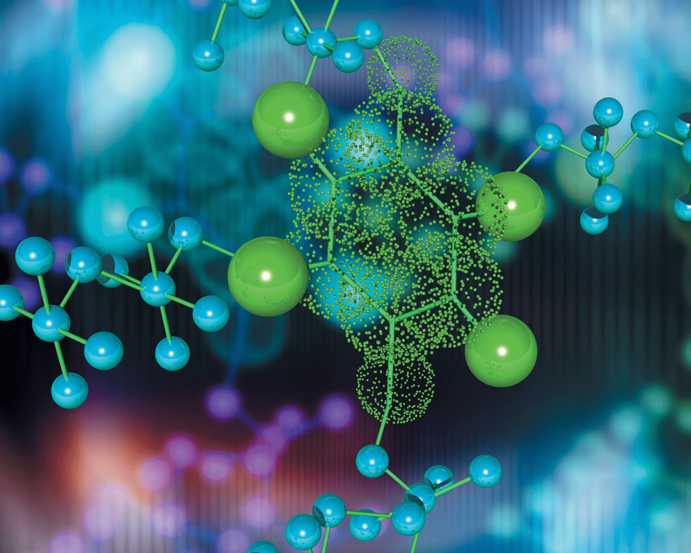
In remote epitaxy, material is still grown on top of a substrate wafer. First, however, the wafer is coated with a layer of graphene. When atoms flow over the graphene-covered wafer, they arrange in the same crystalline pattern as the underlying wafer, but the graphene allows the new material to be removed after formation.
The resulting films display flexibility, and depending on which material they’re made from, they may have other unique properties. At MIT, researchers have found that they can stack films with different crystalline structures and combine them into a multifunctional device by applying heat.
In addition to allowing for flexible, multifunctional computer chips, the remote epitaxy process also allows substrate wafers to be reused. The wafers used in traditional epitaxy can be expensive, so this development could lead to significant cost savings for manufacturers.
Applications for Materials Made Using Remote Epitaxy
By allowing manufacturers to merge previously difficult-to-combine materials and create flexible semiconductors, remote epitaxy may enable us to create a range of flexible electronic devices. For example, researchers have experimented with using remote epitaxy to create films from complex oxides. These compounds have a range of magnetic and electrical properties, and some combinations could generate electricity when stretched or exposed to magnetic fields.
Other potential applications for materials made through remote epitaxy include:
- Virtual reality contact lenses
- Solar power skins for vehicles
- Comfortable electronic fabrics
- Skin-adhering, wireless vital sign monitors
Industries from health care to consumer electronics could be transformed when remote epitaxy processes become mainstream.
Stay Up-to-Date With Developments in Electronics Manufacturing
Remote epitaxy research and experimentation is ongoing, with researchers currently exploring different film combinations and applications. To remain competitive, electronics manufacturers need to monitor developing trends closely and look to the future.
For the latest manufacturing industry news, subscribe to our blog or reach out to us today. At Global Electronic Services, we repair industrial electronics for more than 60,000 manufacturers and distributors worldwide.