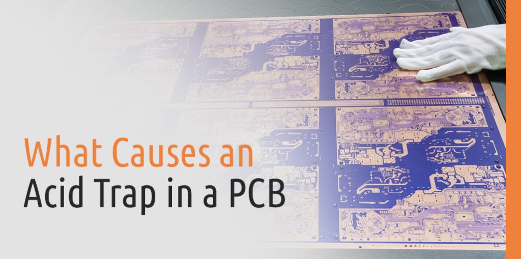
What Causes an Acid Trap in a PCB
What Are PCB Acid Traps
Why Acid Traps Are a Problem
The Cause of Acid Traps
How to Prevent Acid Traps
What to Do If Your PCB Has An Acid Trap
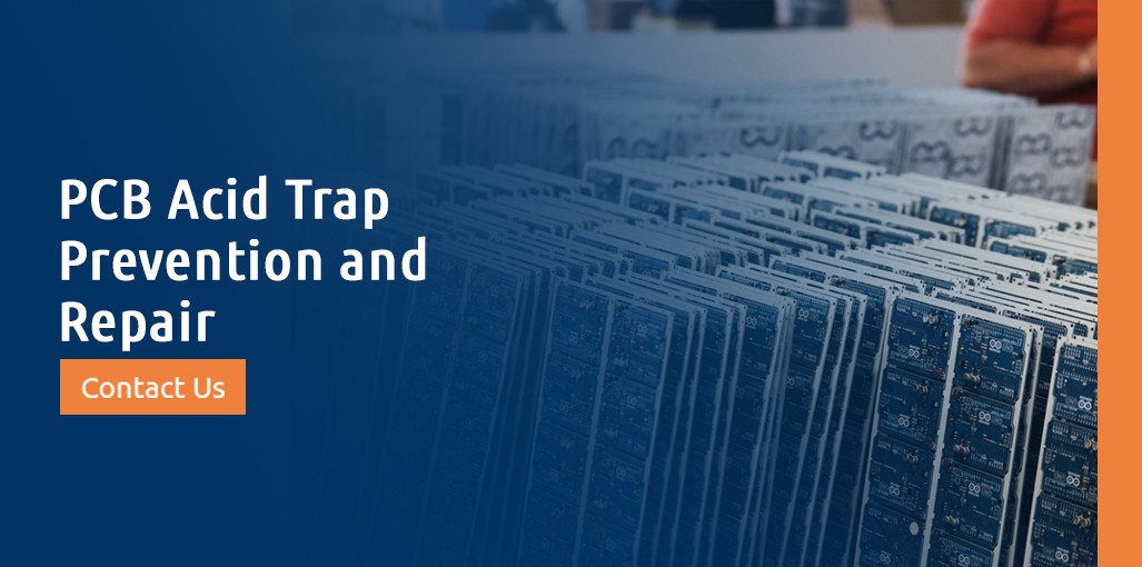
PCB Acid Trap Prevention and Repair
Printed circuit board (PCB) design is no easy task, and one pitfall that your company needs to be aware of is acid traps. These dangerous little spots can open up a PCB to corrosion, open circuits and short circuits. They can wear away the vital copper coatings and affect the conductivity of tracings and components. If you don’t pay attention to acid traps, you may end up with defective circuit boards, wasted material and a project that’s running behind schedule.
Fortunately, there are ways to avoid acid traps. With the help of a detailed eye and various design programs, companies can eliminate some of the most common causes of acid traps in PCBs. We’ve compiled a guide to acid traps to help you further understand their reasons and how to help your team best avoid them.
What Are PCB Acid Traps?
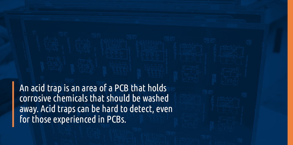
An acid trap is an area of a PCB that holds corrosive chemicals that should be washed away. Acid traps can be hard to detect, even for those experienced in PCBs. Many designers fall victim to them. To understand acid traps, you need to revisit the process by which a PCB is made.
The copper etching process is essential to the formation of acid traps. Most PCB manufacturers use a method with photosensitive chemicals that respond to ultraviolet (UV) light. This approach offers a cleaner result than one with traditional, more aggressive chemicals. If you’re working with a manufacturer that uses traditional chemicals, you’ll have to pay even more attention to the threat of acid traps, as the chemicals make it much easier for corrosion to occur within the acid traps. We’ll talk more about chemical selection later, but know that it will make a difference. For the more common, photosensitive approach, the steps for PCB manufacturing typically include the following.
- After the design is completed, a specialized plotted printer creates a film or negative of the board layout. This film separates the PCB’s design into conductive areas, like copper plating and circuitry, and non-conductive regions such as the base.
- To start creating the physical PCB, a copper layer is bonded to a fiberglass and resin substrate. Then a resist covers the copper. This is a photosensitive film that hardens upon exposure to UV light. The inked film with the design layout goes on top of the photosensitive film.
- When UV light hits these layers, the areas covered with ink from the printed film do not harden. A chemical removal process then washes away these areas, and the unwanted copper is etched away. What exists now is a copper pattern to match the film.
One crucial step in the process of creating a PCB is the stage in which a chemical solution removes the excess copper. An acid trap, of course, traps this corrosive chemical in place, preventing it from washing off. This holding action results in the acid removing areas that should have copper in them, thus disconnecting nodes and circuits. Some design flaws make acid traps more common and dangerous to the rest of the PCB, which is why it’s essential to take steps to avoid them. Corrosion is a substantial danger to PCBs.
Unfortunately, acid traps can sometimes slip by a design rule checking (DRC) test, so designers must stay alert for them.
Why Acid Traps Are a Problem
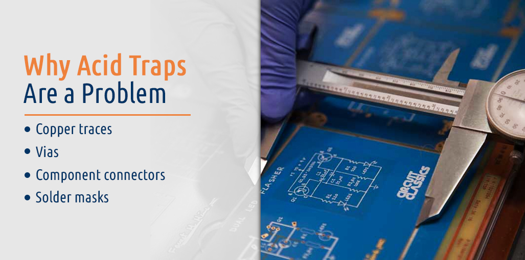
Unsurprisingly, additional deposits of corrosive acid can cause more than one problem for a PCB. It can affect several different components, including:
- Copper traces: As mentioned, a major problem with acid traps is the corrosion of part of the copper trace. When it erodes, you get open circuits. They also lead to issues with connectivity, short circuits and more. As it’s stuck, this acid can seep out of its trap and damage other areas of the PCB. This issue is notorious within acid traps and can cause critical components to malfunction.
- Vias: One of the areas that the acid can seep into is a via. If this happens to vias that aren’t tented, the acid will eat away at them. Designers can minimize the damage if they’ve plugged or tented the vias. Unfortunately, if they are open, the acid can seep over to the other side of the circuit board and damage parts on that end, as well. You may see open traces and damaged components on both sides. Vias that don’t maintain a sufficient distance from each other may be especially susceptible to this kind of damage. One of the ways to reduce the risks associated with acid traps is to keep the vias at sufficient distances from each other.
- Component connectors: Acid that reaches the pads can spell problems for the connectors of different components. The pads are small patches of copper that allow you to solder your component connectors mechanically. If acid reaches this copper, it can erode it and remove it, making it challenging to keep the connection intact.
- Solder masks: Problems with the solder mask are less common, but if acids reach it, damage can occur. When the solder mask is affected, the board is vulnerable to a variety of external factors like oxidation. These outside influences can reduce the lifespan of the board and allow issues to arise more easily. It may also affect the green coating on the board, making it look less attractive.
By disconnecting just one important trace or component, acid traps can pose major threats to your PCBs and the electronics they power. The damage from an acid trap can quickly turn a working PCB into a defective one in several different ways. Plus, acid traps are difficult to fix or remove after the damage is done. The best approach is to prevent acid traps before they appear.
The Cause of Acid Traps
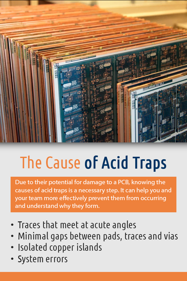
Due to their potential for damage to a PCB, knowing the causes of acid traps is a necessary step. It can help you and your team more effectively prevent them from occurring and understand why they form. The sources behind acid traps include the following.
- Traces that meet at acute angles: Traces that join at particularly acute angles are a frequent culprit for creating acid traps. Acute angles are those under 90 degrees. Even at 90 degrees, sharp corners can pose a significant risk in acid trap formation. Designers typically avoid these and instead opt for a smoother curve. It might sound easy enough to avoid making right or small angles, but they often appear when joining two traces together. They can easily slip by even experienced designers. Take care to avoid these small angles and be aware of the possibility whenever joining traces.
- Minimal gaps between pads, traces and vias: Any space that is too small can lead to acid traps. These gaps are a common way to get a short circuit in the manufacturing process. Extra acid can seep into the traces and cause corrosion to those areas. This trace corrosion is a particular concern if your traces are thin, as there is less copper that needs erosion to open the circuit. Another issue here is that the traces can join together during manufacturing, leading to shorts. Depending on your design, leaving several mils between components is usually enough to eliminate the possibility of acid traps. Most PCB design software can help you by defining this value automatically. Don’t neglect the space between the copper and the edge of the board, either.
- Isolated copper islands: Copper areas that don’t have any real use are called isolated plane islands, copper islands and dead copper. Sometimes, designers leave these copper portions unetched to use fewer chemicals in the manufacturing process. Other times, they slip by unnoticed and unintended. These islands can cause issues regarding signal interference. Plus, they are perfect spots for acid to become trapped in the etching process. Be sure to remove any of these islands. They’re not difficult to get rid of, as many PCB design programs come with options to remove these dead copper areas automatically. It’s an easy fix, so take care to eliminate them to ensure fewer opportunities for acid traps to spring up.
- System errors: In some operations, automated design software is a lifesaver. People working with exceptionally high volumes of PCBs can miss acid trap problem spots and rely on software to help them catch their presence. Unfortunately, these kinds of programs are not perfect. They can still create acute angles and gaps that are too small. Usually, acid trap risks are created when the software’s settings aren’t properly adjusted. Be sure to appropriately define rules before designing. Design rule checking, while typically quite good at catching acid traps, can sometimes miss things too. Always double-check a design after DRC programs run because certain features could spell trouble for a PCB if left in place.
Any area where a hole can collect acid is considered an acid trap. Whether that is a thin gap, an overly sharp angle or extra copper islands, these locations are the perfect spot for acid to hang out in. Know the common areas where acid traps form and keep a watchful eye out for them in PCB designs.
How to Prevent Acid Traps
Though the causes for acid traps are numerous, defending against them isn’t a particularly difficult task, and it’s much easier to do than to fix the effects of acid corrosion. A little basic preparation and care can help your company keep designs free of acid traps and the damage they bring.
1. Ensure Your Design Is Flawless
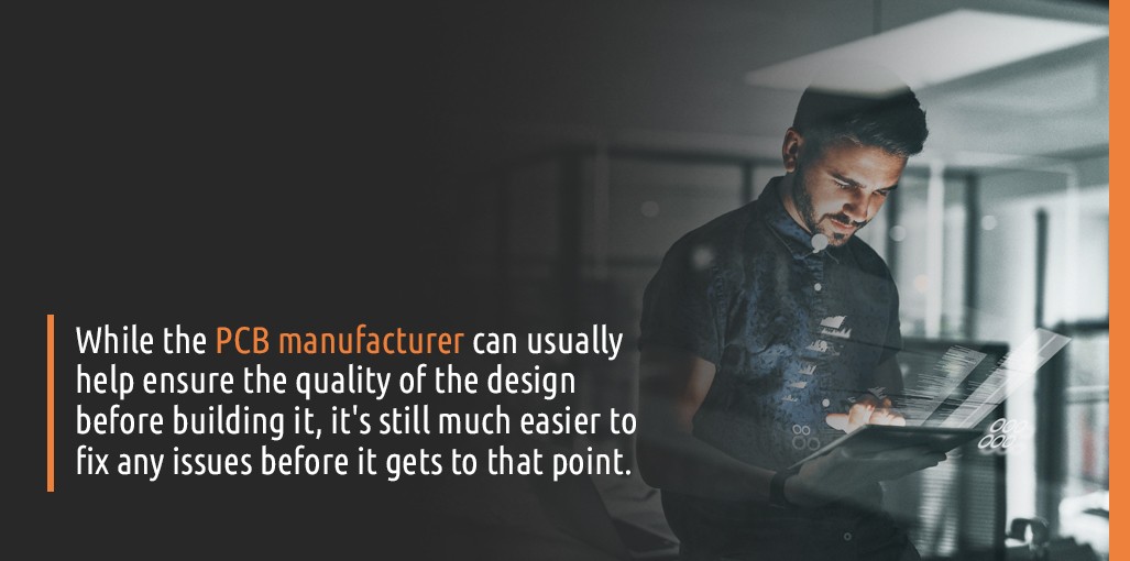
While the PCB manufacturer can usually help ensure the quality of the design before building it, it’s still much easier to fix any issues before it gets to that point. Review the circuit board’s layout carefully and look for acute angles and trace gaps that could create pockets for the acid to collect in. There shouldn’t be any places that could cause problems down the road.
The manufacturer will sometimes run a design through software that tests it for its manufacturability, so they know that the PCB’s layout won’t lead to problems. It may also help to identify PCB design issues that a DRC can’t catch. Your company can also perform this step if you want to be more prepared.
2. Drill More Holes With Extra Vias
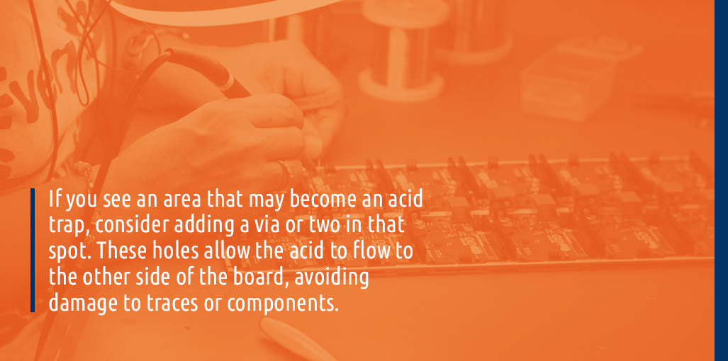
If you see an area that may become an acid trap, consider adding a via or two in that spot. These holes allow the acid to flow to the other side of the board, avoiding damage to traces or components. Of course, this requires caution, so you don’t drill through anything important on either side. Double-layered boards can be tricky in this regard, and this approach is best for single-sided boards.
Watch out for the hazards of group vias. When placing multiple vias close to traces, they can create pockets that become acid traps. Make sure that your design keeps gaps in between vias to space them further apart. They shouldn’t be close to each other or traces. The small amount of board real estate available in PCB design can make this spacing difficult. So increase the gaps if possible.
3. Use Photoactivated Etchants
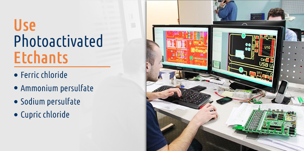
Using photoactivated etchants is one of the easiest and simplest ways to avoid acid traps, and most PCB manufacturers are jumping on this route. It eliminates many of the hazards of acid traps. Traditional etching chemicals include:
- Ferric chloride
- Ammonium persulfate
- Sodium persulfate
- Cupric chloride
The modern approach of using photosensitive films offers many benefits over their predecessors. Though you still need to abide by the PCB etching process, you can minimize the impact of overaggressive chemicals by using the photosensitive approach. Most PCB manufacturers now use more modern procedures that eliminate the use of corrosive materials like ferric chloride and hydrochloric acid. When you use these chemicals, there may be a higher chance of the acid seeping into unwanted areas and corroding more copper. Eliminating these chemicals all together is a great way to avoid their destructive effects.
Photoactivated etchants are those that activate or harden underneath a UV light. They aren’t very reactive unless exposed to the right type of lighting. If the etchant is in a blocked-off area of the board, the lack of light prevents it from causing too much damage. Even thicker layers of copper perform well with photoactivated etchants. They offer cleaner edges and can, therefore, help reduce acid collection in certain areas. These etchants also tend to be less corrosive, so if they become trapped in corners and pockets, they won’t affect the copper as much as traditional chemicals. This method is the one commonly used today as it tends to offer better results.
Working with a fabricator that uses photosensitive films is one of the most significant ways to reduce the risk of acid traps. This chemical aggressiveness is more of an issue for DIY PCB builders, but businesses that operate on larger scales shouldn’t have a problem finding manufacturers that work with modern materials.
4. Run DRC
This step may seem like a no-brainer, but running DRC before submitting a design is a critical step. This software will help you identify issues present on your board. It analyzes your layout against a set of defined parameters to see whether or not the board has those parameters in place. For instance, you can use DRC to check that your trace lines meet a specified width and whether circuits have separate grounds. You can also use it to check that all your angles are properly sized, and there aren’t any small gaps. The DRC step is especially vital if your board is high-density or has multiple layers.
5. Run DFM and Use Modern Manufacturing Methods

Design for manufacturing (DFM) software is an excellent way to check your board for its manufacturability. It improves the ease and efficiency of the manufacturing process, and that includes how it is going to stand up to the etching process. Acid traps, after all, occur during manufacturing. It can also help optimize a board in terms of dimensions and materials, making life a little easier for everyone involved. Running a design through a DFM program can help identify acid trap issues before they cause problems.
Another manufacturing consideration involves the modernity of your manufacturer’s process. Using photosensitive chemicals is one indicator of their practices. Learn about their manufacturing technique and assess whether it works for your needs. PCB design has come a long way, so make sure your manufacturer has kept up with the times.
5. Double Check Your Work
Even running DRC can’t catch everything. Plus, human errors are common. Like spellcheck, you can’t depend on the DRC to find all errors in your work. Go over your design carefully, looking out for any of the pitfalls we’ve mentioned. It may be an extra step, but spending a little more time and effort here can offer significant savings in fixing errors and defective PCBs. It may even help to have another designer take a look to get a second pair of eyes.
Catching acid traps before your board reaches the manufacturing stage is crucial to minimizing wasted operational costs and getting boards printed on schedule. If circuit boards get printed with acid traps in place, you end up with a bunch of defective boards. Taking steps to eliminate acid traps before they reach manufacturing can save you a lot of headaches down the road and make the process smoother for both your company and the manufacturer.
What to Do If Your PCB Has an Acid Trap
While prevention is always better in this case, all hope is not lost if you find an acid trap in your PCB.
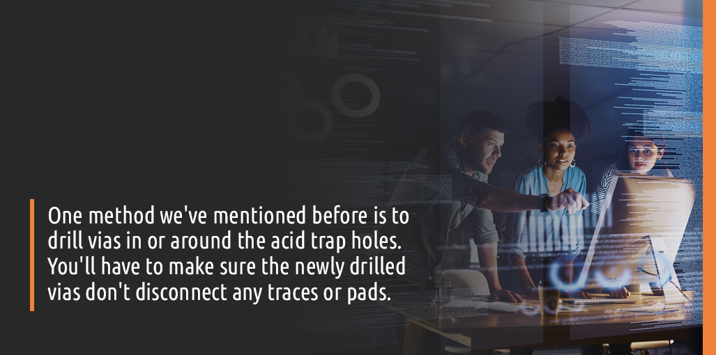
One method we’ve mentioned before is to drill vias in or around the acid trap holes. You’ll have to make sure the newly drilled vias don’t disconnect any traces or pads, but this method can let the acid leave the circuit board without damaging more components. It is best to drill vias for single-sided PCBs.
Of course, that approach won’t work for all designs. You may have to take more aggressive measures to fix problems from acid traps. If your layout hasn’t been printed yet, you can always adjust the design files. Remember that many PCB design programs offer automated features for removing acute angles and isolated copper islands. Take advantage of these to get rid of acid traps in the design stage.
If none of these are options, you may need to look into professional repair. Industrial-level PCB repair can offer more expertise and help from a dedicated repair center.
PCB Acid Trap Prevention and Repair
Acid traps are just one more element of PCB design that your team will need to be aware of. The acidic corrosion can damage traces, components, vias and more, making them a serious concern for any circuit board. Thankfully, with careful design strategies, like avoiding acute angles and ensuring sufficient gaps between traces and vias, you can successfully prevent acid traps.
Sometimes, despite everyone’s best efforts, acid traps still make their way into a final product. If this happens and your company can’t repair it, you may be able to enlist the help of a professional repair service. Global Electronic Services repair offers industrial electronics repair throughout the United States. Request a quote today for more information on PCB repair options.