Guide to Troubleshooting PCBs
How to Troubleshoot Printed Circuit Boards
Printed circuit boards (PCBs) are manufactured according to designer specifications. However, errors can occur during the construction process, or accidents happen along the way that render them faulty. In either case, it is sometimes necessary to repair a malfunctioning circuit board or perform some other maintenance.
Whether you need to repair circuit board trace, repair a PCB pad or rectify some other issue, it is crucial to understand the intricacies of circuit boards. For starters, a few basic facts about electricity should be covered.
Electricity
The charge of electricity powers everything from lights, appliances and stereos to computers and factory equipment. Electricity itself is merely embodied by electron flow, which generally passes from an upper to lower level. As such, electrical currents always travel from a positive to negative level of voltage from the current source.
In electrical circuits, the principal elements are the current and voltage, as well as the capacitors, inductors and resistors. There are two types of electrical current — alternating current (AC) and direct current (DC). An AC current is in the form of a curve, or sine wave, while a DC current is in the form of a straight line.
In hardware circles, the process of circuit board development — in which the various components that comprise a circuit are assembled into place — is known as PCB design.
Printed Circuit Boards
For the majority of electrical boards, the name “printed circuit board” is used, or “PCB” for short. In the past, PCBs were manufactured through a complex process that consisted of detailed wiring on specific points. During this process, the circuits were left exposed and hence vulnerable to damage. It was only with the development of safer, more advanced design methods that the process reached the standards of security that are used in PCB manufacturing today.
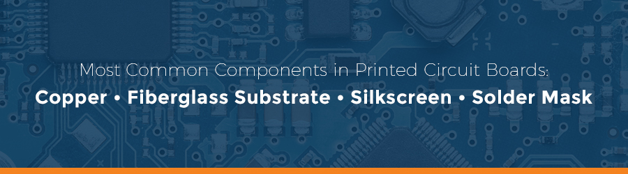
The following four components are present on most of today’s printed circuit boards — copper, fiberglass substrate, silkscreen and solder mask. In the earlier years of the technology, PCBs consisted of one layer. By contrast, contemporary PCBs consist of multiple layers, which are necessary to accommodate today’s complex circuitry.
In newer PCBs, numerous high-pitch parts are included but not identified on the boards. Consequently, the methods required to troubleshoot and repair today’s PCBs is more complicated than ever. On circuit boards of the 1980s and ’90s, it was possible to perform repairs with the use of automatic testing tools, which simply do not work on today’s PCBs.
Troubleshooting on Old PCBs
On older printed circuit boards, the techniques used for troubleshooting were performed in a variety of ways, including the following:
- Inspection of the solder joints
- Identification of the problem
- Troubleshooting of specific parts
- Inspection of the integrated circuits
- Consultation of the software manual
- Inspection with a microscope
- Tests of the functionality
The majority of these tests are ineffective at troubleshooting the types of problems that occur on newer printed circuit boards. In response to these newer challenges, today’s PCBs receive a more complex analysis.
Analogue Signature Analysis
A component can be tested with the use of two probes and a sine wave. On the liquid crystal display (LCD), you will see the voltage, currents and phase shifts. The current is on the y-axis, while voltage is on the x-axis, you can see the resultant trace on the LCD screen.
How to Diagnose Problems With a PCB
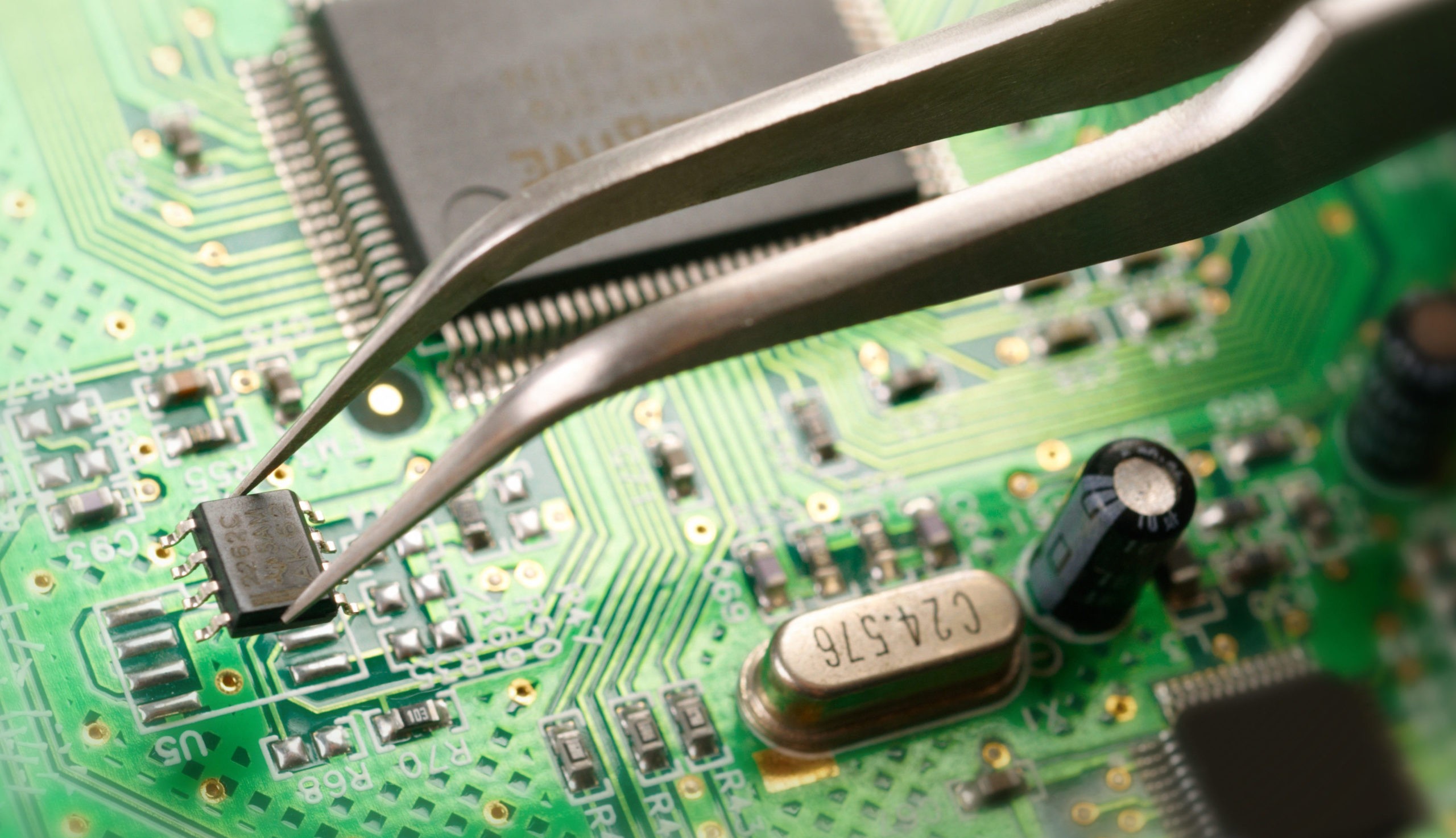
Before you actually go about with repair work on a printed circuit board, you must first pinpoint the root of the problem. Diagnostic work on a faulty PCB is carried out in the following stages:
- Identify the problem with the use of a VI instrument. The alternating voltage is used to test the unidentified pin count.
- The next step is to identify the location of the problem. This requires examinations at a microscopic level to find the troubled elements.
Lastly, the faulty part is removed from the circuit board, and a replacement part is put in its place.
How to Analyze the Results of PCB Diagnostics
The components in an electrical circuit are arranged in one of the following three combinations — mixed, parallel or series. Since it is usually impossible to pinpoint the signature, the easiest way to approach an analysis is to compare the faulty PCB with a functional one of the same make. This way, you can see the common signatures.
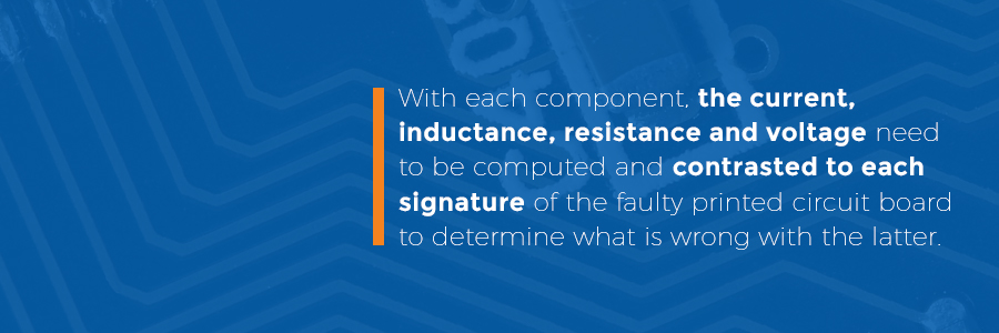
To compare signatures, you must examine the similarities between all defective printed circuit boards and then contrast those to the PCBs that are free of problems. With each component, the current, inductance, resistance and voltage of each component needs to be computed and contrasted to each signature of the faulty printed circuit board to determine what is wrong with the latter.
Clear away deposits of dry or partially worn off solder if any is present on the faulty PCB. This will refresh the points and make it easier to inspect the signature.
With the numerous amount of tracks on a printed circuit board, there is a high likelihood that certain tracks will incur damage during the examination process. To remedy any damage that results during these steps, jumper wire is a helpful tool for track repair.
During the final step, each pin is tested to determine its functionality. If the output and input of a pin conform to the specs of the data sheet, that means the pin is in good condition. If not, it must be removed.
How to Fix a PCB
When a device is disconnected from a PCB, pads will often get damaged as a result. This is because the PCB and circuit frame library share joined traces which are cut from one another when a device is removed from a printed circuit board. However, it is possible to fix the affected SMT land/trace combinations.
When you sit down to fix a printed circuit board, you should have the following materials at hand:
- C-clamps (small)
- Circuit frame
- Dental picks
- Flux
- Isopropyl alcohol
- Kapton™ tape
- Knife
- Microscope
- Orange sticks
- Solder
- Soldering iron
- Wipes
Additionally, you need an ESD-safe surface for cutting.
Steps to Fix and Troubleshoot PCBs
Step #1. Clean the PCB
Use isopropyl alcohol to clean the affected part of the PCB. Once the area is clean, dry away the alcohol with compressed air.
Step #2. Take off the Damaged Pad
Use an Exacto knife to gently peel off the damaged, pre-existing pad.
Step #3. Clear Away Laminate Around the Pad
If you see any burnt laminate on the area in question, be sure to remove it before you proceed.
Step #4. Remove Old Solder Mask
Take a dental pick and use it to eliminate lingering solder mask on the conductor.
Step #5. Clean With Alcohol
With isopropyl alcohol, wipe the spot and blow it dry with compressed air. Alternately, you can use a cloth as long as it has no lint.
Step #6. Prepare the Conductor
With proper solder alloy in hand, prepare the conductor area on the spot where the replacement conductor will be affixed.
Step #7. Examine and Choose the Appropriate Circuit Frame
From the available choices on the circuit frame, choose your new conductor. Remove your selection from the circuit frame with a small knife.
Step #8. Prepare the New Pad/Conductor
With a suitably alloyed solder, cover the spot on the new conductor that will face the old trace. Next, prepare your epoxy. Given that the epoxy will only be good for about 45 minutes, it is best to prepare only small portions at a time. Apply the epoxy mixture to the printed circuit board. To speed up the bonding process, place in open air. You can also cure the joined pieces in an oven.
Step #9. Solder the New Pad/Trace to the Old Conductor
Using Kapton™ tape, put the new conductor into place.
Step #10. Hold and Dry
Clamp the new pad in its spot for the duration of time that it takes to cure. Once finished, take off the clamp. At this stage in the process, it is also wise to conduct a brief inspection of the electrical continuity. It might also help to place solder mask around the pad edges and allow it to dry for additional strength.
Common Issues With PCBs
To repair a PCB pad or another circuit board component, you must first pinpoint the problem. There are several manufacturing defects possible that can render a PCB faulty, including the following:
Issue #1. Plating Gaps
Electricity passes from one end of a PCB to the other through holes coated with copper, also known as plated thru-holes. These holes are formed with fabricator drills, which manufacturers use to carefully puncture the surface of circuit boards. An electroplating process is then performed to line each hole with copper.
Even though the process is generally reliable, it can have its imperfections. If difficulties occur while the deposition is in progress, it could result in gaps along the plating. This can render the PCB worthless because electricity won’t pass if gaps in the copper are present.
Gaps are typically formed by the presence of air bubbles or contaminants during the deposition process. Plating gaps can be prevented if the newly drilled PCB board is properly cleaned in advance of electroplating. Furthermore, it is important for makers to pay close attention to the movement of the drill as the hole is being created.
Specifically, there is a certain number of drill hits to be performed at a specific speed, and anything outside those specifications could damage the circuit board. As such, it is crucial to hire the services of an advanced, reputed PCB maker when you need printed circuit boards.
Issue #2. Raw-Cut Copper at the Edge
The high conductivity of copper makes it an ideal metal for printed circuit boards. That said, copper does have its weaknesses, namely its softness and susceptibility to rust. To safeguard copper from the external effects that can lead to corrosion on a copper surface, the metal needs to be coated with a protective material.
However, despite the protective intent of copper coating, if copper is exposed at the edge while a circuit board undergoes the trimming stage, the copper will get cut and left exposed without that coating. More dangerously, if two raw copper planes come into contact and touch a conductive material at the same time, a short will result. A PCB in this state is also liable to emit an electrical shock upon contact.
Issue #3. Slivers
When PCBs undergo the fabrication process, thin slivers of solder mask or copper are among the possible byproducts. There are two scenarios that allow for these wedges to form:
- If long strips of copper are etched and a sliver comes undone before enough time has passed for it to dissolve. The sliver could possibly fall into a chemical bath and get passed onto another board.
- If a portion of a printed circuit board is cut either too wide or too narrow.
Either possibility could seriously corrupt the functionality of a PCB. Slivers can leave plating exposed that would otherwise be protected with solder mask. Alternately, slivers could end up connecting two different sections of copper. Both scenarios are liable to reduce the life of a printed circuit board.
Issue #4. Incomplete Solder Mask Between Pads
The layer above the copper on a PCB is the solder mask. The purpose of solder mask is to keep the copper safeguarded from foreign metals or conductive elements. Solder mask also protects the copper from potentially corrosive exposure to the environment. Furthermore, solder mask protects handlers from the possibility of electrical shock.
There is a part of the metal that is left exposed on a circuit board. This is known as a pad. The pad is where foreign parts are soldered to during the assembly of a PCB. However, solder mask is sometimes either incomplete or missing entirely between two facing pads. In addition to leaving copper exposed, this can create unintended contact between pins.

Incomplete or missing solder mask is typically the result of a manufacturer’s oversight. If the application dimensions for solder mask are miscalculated during production, pad holes are bound to be incorrectly sized, thus rendering the PCBs unusable.
Issue #5. Acid Traps
When acid is captured at narrow angles in a circuit during the etching phase of PCB production, the problem is known as an “acid trap.” Due to the acute angles of such traps, the acid is held longer than necessary. Consequently, the acid can render a circuit defective and lead to further issues down the line. In most cases, acid traps occur when oversights are made during production.
Issue #6. Starved Thermals
Thermals are placed around pads to disperse heat. As a board undergoes the soldering process, thermals play a critical role. However, if a thermal is applied inconsistently, the PCB could ultimately have connectivity issues.
Insufficient thermals stall the process of heat transference between the pads and planes. This, in turn, can make it difficult to solder a board correctly. When constructed under these conditions, the PCB is liable to overheat once it is put to use. However, experts can diagnose and correct this potential problem.
PCB Repair
Printed circuit board repairs are best handled by skilled technicians. At Global Electronic Services, we stock hundreds of thousands of components to provide fast and thorough PCB repairs. Contact GES for PCB repair services today.